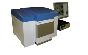
Novelx has been selected as the runner up for a Wall Street Journal Technology Innovation Award in the Materials and Other Base Technologies category.
The journal recognised Novelx for using silicon-processing technologies to miniaturise the core technology inside a scanning electron microscope (SEM).
Powered by Novelx Stacked Silicon Technology, the Novelx mySEM is a bench-top SEM for imaging and characterising nanoscale objects and materials.
In a compact design that installs easily into available lab space or closer to production lines, the mySEM delivers capabilities previously only available in high-end field emission SEMs.
Optimised for low-voltage operation and without the need to coat non-conductive samples, the mySEM is suitable for the imaging of energy-sensitive nanomaterials, biomaterials, polymers, thin films and membranes.
This year, judges considered whether application of entries would be particularly useful in a time of economic hardship.
Jim Rynne, vice president of business development at Novelx, said: 'The mySEM will make nanoscale imaging more accessible by distributing high-resolution and low-voltage imaging capabilities more broadly and cost-effectively.
'The market timing for such a solution is ideal as the size of silicon features continues to shrink according to Moore's law and the number of new product innovations incorporating nanomaterials increases.
He added: 'The imaging capabilities of the mySEM are needed to both speed new product development cycles and to move nanoscale quality assurance closer to production lines.' Industrial applications include the characterisation of nanomaterials at corporate product development labs, the failure analysis of nanoscale defects and the quality assurance of products designed with nanomaterials.


