'Super-resolution' microscope for nanostructures
1 May 2013

Researchers have found a way to see synthetic nanostructures using a new type of super-resolution optical microscopy.
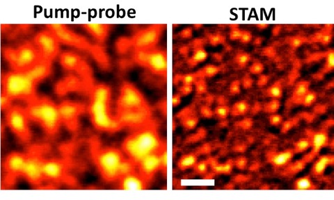
The imaging system developed at Purdue University is called saturated transient absorption microscopy, or STAM.
It uses a trio of laser beams, including a doughnut-shaped laser beam, that selectively illuminates some molecules but not others.
[The technique] has great potential for the study of nanomaterials, both natural and synthetic
Electrons in the atoms of illuminated molecules are kicked temporarily into a higher energy level and are said to be excited, while the others remain in their “ground state.”
Images are generated using a laser called a probe to compare the contrast between the excited and ground-state molecules.
“Here, we demonstrate a new scheme for breaking the diffraction limit in optical imaging of non-fluorescent species. Because it is label-free, the signal is directly from the object so that we can learn more about the nanostructure,” explained Ji-Xin Cheng, an associate professor of biomedical engineering and chemistry at Purdue University.
The researchers demonstrated the technique, taking images of graphite “nanoplatelets” about 100 nanometers wide.
“It’s a proof of concept and has great potential for the study of nanomaterials, both natural and synthetic,” Cheng said.
The doughnut-shaped laser excitation technique, invented by researcher Stefan Hell, makes it possible to focus on yet smaller objects.
Researchers hope to improve the imaging system to see objects about 10 nanometers in diameter, or about 30 times smaller than possible using conventional optical microscopes.
“We are not there yet, but a few schemes can be applied to further increase the resolution of our system,” Cheng said.
Future research may include work to use lasers with shorter wavelengths of light. Because the wavelengths are shorter, the doughnut hole is smaller, possibly allowing researchers to focus on smaller objects.

