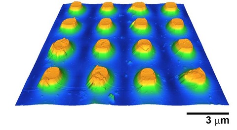
A study from the University of Illinois has described the effects of nanometer-scale heating on semiconductor plasmonic microparticles.
The research team measured nanometer-scale infrared absorption in semiconductor plasmonic particles.
The technique combined atomic force microscopy (AFM) with infrared spectroscopy, explained William P King, an Abel Bliss Professor at Illinois.
“Atomic force microscope infrared spectroscopy (AFM-IR) allows us to directly observe the plasmonic behaviour within microparticle infrared antennas,” added King.
Daniel M Wasserman, assistant professor at Illinois, stated that: “Highly doped semiconductors can serve as wavelength flexible plasmonic metals in the infrared,” adding, “without the ability to visualise the optical response in the vicinity of the plasmonic particles, we can only infer the near-field behaviour of the structures from their far-field response.”
Professor Wasserman explained that the research indicated a clear window into the optical behaviour of a new class of materials on a length scale much smaller than the wavelength of light.
The article which described the technique, ‘Near-field infrared absorption of plasmonic semiconductor microparticles studied using atomic force microscope infrared spectroscopy’, appears in the publication, Applied Physics Letters.
The article compared near-field and far-field measurements that confirmed the presence of localised plasmonic resonance.
Jonathan Felts, of the Illinois research team, suggested that: “We can now measure the optical behaviour of individual features, and can start to think about designing and testing more complex optical materials.”
The research was conducted using an Anasys AFM-IR imaging instrument.


