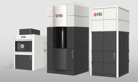
FEI has launched three systems that tailor the power of transmission electron microscopy to specific application.
The systems are designed to provide efficient and effective application-specific workflows for semiconductor manufacturing and scientific research.
They include the Metrios TEM for advanced semiconductor manufacturing metrology, Talos TEM for high-speed imaging and analysis for materials and life sciences applications, and the Titan Themis TEM for enhanced atomic-scale measurements of material properties.
“With these three systems we have now introduced an unprecedented total of six new TEMs in the past year,” said Benjamin Loh, FEI’s executive vice president and chief operating officer.
“All six have been designed and built to provide an application-specific workflow that delivers contextual information of immediate value to users in science and industrial market segments, including materials science, chemicals, life sciences, and semiconductor manufacturing. Our goal is to completely change the world of TEM so our customers can change their world as well.”
The Metrios system is claimed to be the first TEM dedicated to providing the fast, precise measurements that semiconductor manufacturers need to develop and control their wafer fabrication processes.
Extensive automation of the basic TEM operation and measurement procedures minimises requirements for specialised operator training. Its advanced automated metrology delivers greater precision than manual methods. The Metrios TEM is designed to provide customers with improved throughput and lower cost-per-sample than other TEMs.
The Talos TEM combines high-resolution, high-throughput TEM imaging with fast, precise and quantitative energy dispersive x-ray (EDX) analysis to deliver advanced analytical performance with class-leading value.
The TEM is available with FEI’s highest brightness electron source and latest EDX detector technology to provide high-efficiency detection of low concentration and light elements, along with FEI’s 3D EDS tomography.
Excellent performance at lower accelerating voltages permits the use of lower beam energies to reduce sample damage on delicate materials. The Talos platform is completely digital, allowing for remote operation and it also enables the addition of application-specific detectors or sample holders for dynamic experiments.
With enhanced automation and ease-of-use, the Talos is especially well-suited for the individual investigator as well as multi-user laboratory environments.
The Titan Themis TEM extends FEI’s leadership position in aberration-corrected, atomic-scale imaging and analysis. Researchers use the high resolution of aberration-corrected TEM to understand relationships between a material’s larger-scale physical properties and its atomic-scale composition and structure.
The Titan Themis platform enables direct measurements of properties, such as magnetic fields, on the nanometer-length scale and electric fields even down to the atomic scale.
Automation of the complete TEM workflow, from sample navigation and alignment through final data acquisition, enhances the repeatability and reproducibility of results to enable more confident conclusions with less time and effort.


